19.08.2025
47 min
657

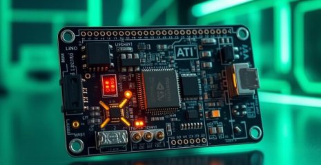
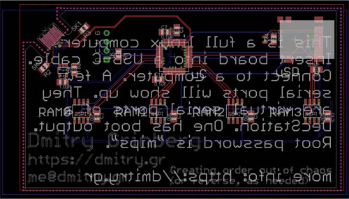
LinuxCard is a unique DIY project where a regular business card-shaped printed circuit board can run a full-fledged Linux. The author used an ATSAMD21 microcontroller, external memory, and a microSD slot to recreate the work of an old DECstation on minimalist hardware. Thanks to this unconventional approach, it was possible to load the Linux kernel in just a few minutes and get a working shell directly from the business card. The project shows how you can build an impressive emulated computer from available components that can run basic programs, compile code, and even boot other OSes, such as Ultrix. LinuxCard is an example of engineering creativity and proof that Linux can run on almost anything.
A long time ago (in 2012), I ran Linux on an 8-bit AVR. At the time, that was a pretty cool record. I don’t think anyone has ever broken it — no one has managed to run Linux on a device lower than that 8-bit AVR. The main problem was that it was too slow to be practical. The effective speed was 10 kHz, and the boot time was 6 hours. That’s cool, but I doubt any of the people who built one of those devices based on my design ever waited for the device to boot more than once. It was time to improve it!
So what could I improve? A few things. First, I wanted the new design to be fast enough to boot in a few minutes and respond to commands in seconds. That would make using the device practical, not a test of patience. Second, I wanted it to be easy for anyone to assemble. This meant no components with densely packed pins, no components with too many pins, and no components with pins hidden underneath them. Part of that desire was also that someone could actually build it, which meant I had to choose components that were actually available to buy amidst the current shortage of, well, everything. I also wanted the device to be easy to interface with. The original design required a USB-to-serial adapter. That was impossible. And finally, I wanted it all to be cheap and small enough to serve as my calling card.
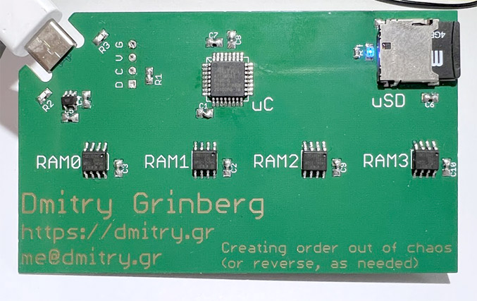
Some things were pretty easy to decide. For example, microSD was perfect for storage — it’s easy to interface, widely available, and cheap. I went with a simple microSD slot that’s easy to solder and easy to buy: the Amphenol 1140084168.
Some of the options were a little more complicated, but not too much. For example, I definitely wasn’t going to use DRAM again. It requires too many pins, which requires more soldering than I would have considered acceptable, given that I wanted this device to be easy to assemble. Megabyte-sized SRAM doesn’t really exist. But there’s this cool thing called PSRAM. It’s basically DRAM, but in a simplified way. It takes care of all the updating itself and acts just like SRAM on the outside. Okay, cool, but it’s still usually a lot of pins. Right? There are “AP Memory” and “ISSI.” They make QSPI PSRAM chips in nice SOIC-8 packages. AP Memory has models with 2MB and 8MB of RAM per chip, ISSI has them in 1MB, 2MB, and 4MB. I decided to use these. They are available, and my code supports them all!
There were a few different options, such as which regulator to use. I chose the MIC5317-3.3YM5TR because I had worked with it before and it was in my “random chips” box. It is also easy to buy.
The USB connector was also an interesting choice. I settled on: none. With the right thickness of the PCB, you can bend the edge of the board so that it fits into the end of the USB-C cable. I had already seen it done for micro-USB, and I thought it could be done for USB-C. In the end, I didn’t even have to do it, because someone else had already saved me the 30 minutes it would have taken. I just had to remember that the board had to be 0.8 mm thick for it to work.
The last choice was the hardest – which microcontroller to use. The criteria were: embedded USB, no more than 32 pins with a pin spacing of at least 0.65 mm, no contactless packages, real availability for purchase, QSPI support, as soon as possible. I didn’t get my last two wishes. After a long search and filtering by the query “in stock”, I was forced to stop at the ATSAMD21 series chip, namely the ATSAMDA1E16. It is not fast (according to the characteristics of 48 MHz, I clock it at 90 MHz), has many errors (especially in the DMA mechanism), but it can be bought, it is easy to solder, and you will have to… UPDATE: now another chip is supported, see further in this article.
I could just take my old ARM emulator (uARM) and use it. But what’s the fun in that? I decided to pick a new target. The ideal target for emulation would be: (1) be a RISC chip so I would have to spend fewer cycles decoding instructions, (2) have no condition codes (like MIPS) or only set them on demand (like ARM) so I wouldn’t waste time calculating them in every virtual cycle, (3) be 32-bit because 16-bit machines are just a piece of cake and 64-bit is hard to emulate, (4) be well-known, and (5) have a working set of GNU tools and Linux userspaces available. This set of requirements really leaves only a few candidates: PowerPC, ARM, MIPS. I’ve been working with ARM and didn’t want to mess around with a byte-shifting processor, so I chose MIPS! Hence the internal project name: uMIPS.
MIPS is an old chip, one of the original RISC designs. If you’re a RISC-V fan, MIPS will look familiar—it’s where 99.9994% of the original RISC-V specification was copied from. The original MIPS had a 32-bit design optimized for ease of design. It has (and doesn’t hide) a delay slot, has many registers, including a hardware-programmable zero register, and doesn’t use condition codes. The original design was the R2000, back in 1986, followed soon after by the improved R3000 in 1988. These were the last chips to implement the MIPS-I instruction set. MIPS-II was short-lived, and only included the R6000, which barely saw the light of day. The real successors were the MIPS-III R4000 series chips released in 1991. They were already 64-bit in 1991! Of course, the easiest target would be the R2000/R3000 chips with their simple MIPS-I instruction set.
MIPS-I is a fairly simple instruction set. So much so that a complete emulator consisting only of instructions can be written in less than 1000 lines of C code without any dirty tricks. The floating point unit is optional, so it can be omitted (for now). The MMU is an odd choice. It’s just a TLB that the software has to fill in manually. This may seem like a rather unusual choice, but it’s actually a smart approach if you’re living in 1986 and trying to minimize the number of transistors on your chip. Why use a hardware page walker when you can have software do it? You might ask, how does it handle the situation when the code that does the page lookup isn’t itself mapped? Well, a portion of physical memory is always hard-mapped at a specific address, and all exception handlers are there. Even if that weren’t the case, since software manages the TLB, it wouldn’t be hard to reserve an entry for this purpose. The hardware even maintains some “wired” entries that are intended to be used continuously. More on all of this later.
The MIPS R2000/R3000 is a processor. A processor does not make a complete system. What system should I emulate? I looked for a cool system and settled on the DECstation2100 (or its big brother, the DECstation3100). Why bother? It seemed like a simple system that Linux could support. I didn’t initially plan to emulate everything. Why? I didn’t plan to emulate the LANCE network adapter or the SII SCSI adapter. The last part might surprise you, since we need a disk that we will use as the root file system. I later added emulation of both of these parts to please Ultrix.
MIPS is a fairly old instruction set, which shows up in a few places. The main one is that it tries to prevent signed overflow. The usual instructions used for addition and subtraction actually throw an exception if they overflow. This doesn’t fit the way processors are used today, so no one cares, but I had to emulate it anyway. There are “unsigned” versions of the instructions for addition and subtraction that don’t do this, and that’s what all modern MIPS compilers produce.
I originally wrote a CPU emulator in C to allow for easy testing on my desktop while the PCBs were being made. It wasn’t fast, and wasn’t intended to be fast, but it did allow for testing. You can see that emulator in cpu.c. Along the way, I implemented some of the R4000’s features at will. It turns out that this is necessary to boot Linux compiled by modern compilers, because the compilers assume these instructions exist. Technically, this is a bug. Realistically, I’m probably the only person who noticed this. So what features did I need to add? Probably branches (BxxL instructions), conditional traps (Tcc/TccI instructions), and atomic traps (LL/CC instructions).
Of course, C is not the language you use when you want to work fast. I also wrote an emulator in assembly language targeting ARMv6-M (for my chosen Cortex-M0 microcontroller). Later I added some improvements for ARMv7-M (in case I ever upgrade the project to a more powerful processor). This was tested on Cortex-M7 and worked well too. The core of the assembly language emulator is in cpuAsm.S, and the ARMv6-M specific parts are in cpuM0.inc.
I mentioned delay slots earlier. What is a delay slot? Well, it used to be cool to open up the processor pipeline to the world. Just kidding, this was just a way to save a few more transistors. Essentially, the instruction after the jump will be executed even if the jump happens. This is called a delay slot. A naive way to avoid this is to put a NOP after every jump instruction. But with a good compiler, a delay slot can be put to good use in almost all cases. Obviously, you can’t put a jump instruction in a delay slot, because the processor is already jumping somewhere. Doing so is illegal and undefined. However, a problem arises if an instruction in a delay slot throws any exception. The processor will record that the instruction was in a delay slot and point the exception handler to the jump whose delay slot we are in. There is no way to get back to this “in a delay slot” state, so the exception handler is expected to take action to somehow execute the delay slot instruction and then complete the jump.
DECstation came with an FPU to make floating point operations fast. Back then it was a separate chip that was optional on the MIPS R2000/R3000 system. Linux will actually emulate the FPU more or less correctly if it’s not there, but it’s slow. I initially used this mode and even fixed a few bugs in the Linux emulation, but eventually I implemented an FPU emulator. This was necessary because many of the MIPS binaries I could find seem to assume that the FPU is available and use it freely. I never reimplemented the FPU emulator in assembler, instead calling the C FPU emulator when needed. I find that squeezing a few cycles out of each instruction doesn’t make sense when the actual FPU operation takes hundreds.
The code for this is in fpu.c. I’m adding Linux patches to remove FPU emulation support from the kernel. This saves some RAM. Later I also added support for a “minimal” FPU – it supports registers but not operations. This is allowed by the specification because the FPU can refuse to perform any operation that it “is not sure it can perform perfectly correctly”, so any compatible OS must implement a full fallback FPU anyway. Why? This saves 16 KB of code in the binary, opening up the possibility of running uMIPS on smaller devices.

(this is a very simplified explanation, feel free to skip it if you know it, and don’t complain to me that it’s not completely accurate!)
Most processors access memory using virtual addresses (VA). Hardware works in terms of physical addresses (PA). The ability to map one to another is the basis of memory security in modern operating systems. The purpose of the MMU (memory management unit) is to translate virtual addresses into physical addresses to ensure this mapping. This is usually done using a tree-like structure in RAM called a page table. Most processors have a component whose job is to traverse this structure to determine which physical address a given virtual address corresponds to. This component is the page table traversal. In most cases, the page table has 3 or 4 levels, which means that to translate a VA to a PA, you need to read 3 or 4 words from main memory. Obviously, you don’t want to make 3 unnecessary memory accesses for every useful one. Therefore, usually another component is included in the MMU – the TLB (translation lookaside buffer). Essentially, you can think of the TLB as a cache of some of the contents of the current page table. The idea is that before performing these 3-4 reads from memory into the page table, you can check if the TLB has a matching entry. If so, you can skip the page table traversal.
It is clear that, like any cache, the TLB needs to be in sync with what it caches (the current page tables). Therefore, if the OS modifies the page tables, it needs to flush the TLB, as it may contain outdated entries. Usually, TLBs provide very little interface to the processor, so there is no way to read all the entries and remove only the new invalid ones. Also, it would be slow, so it is usually not done. However, invalidating the entire TLB also has its costs – it needs to be refilled, which results in 3-4 memory accesses per write. This can be detrimental to performance. A solution called ASID is commonly used.
What are the four main cases where page tables can be modified? (1) Adding a new mapping over a virtual address that was previously unmapped, (2) changing permissions on an existing mapping, (3) removing a mapping, and (4) completely changing the memory map (e.g., to switch to a completely different process). In case 1, no TLB flushing is needed because there cannot be any stale TLB entries. Cases 2 and 3 do require TLB flushing, but they are not as common. However, case 4 is quite common. This is done on every context switch. It might be noted that since we are changing the entire memory map, the entire TLB will be invalid, and therefore flushing it is not a problem. This is incorrect. In addition to mapping user space items, the MMU also maps various kernel structures, and there is no point in penalizing them.
If we could somehow mark which entries in the TLB go to which process, and temporarily disable them when another process is running, we could avoid a lot of context flushing and the performance overhead associated with that. It would also be cool if we could mark entire entries belonging to the kernel and valid in every process. Well, this is exactly the technology that exists in many MMUs. The idea is that each page table entry will have a bit that marks it as “global” (valid in all memory maps) or not. There should also be a register in the processor that sets the current ASID (address space identifier). When the TLB entry is filled from the page tables, the current ASID is written into it. When the TLB is searched, only entries that match the current ASID or those marked as “global” will be matched. Cool!
The idea at the time was to save transistors. Which of the above could be cut? Well, eliminating the TLB guarantees terrible performance in all cases. But do we really need this page table crawler? What if we had software do it? We could add a little help, like being able to efficiently manage the TLB but skip the hardware page table crawler. That’s what MIPS did. Here’s the MIPS virtual address space:
Адреси Зіставлення назв 0x00000000..0x7fffffff kuseg зіставлено через MMU 0x80000000..0x9fffffff kseg0 зіставлено з фізичним 0x00000000..0x1ffffffff, кешовано, якщо кеш є, доступно лише в привілейованому режимі 0xa0000000..0xbffffffff kseg1 зіставлено з фізичним 0x00000000..0x1ffffffff, не кешовано, доступно лише в привілейованому режимі 0xc0000000..0xffffffff kseg2 зіставлено з MMU, доступно лише в привілейованому режимі
So, as you can see, some virtual devices are not mapped through the MMU at all. This means that code that resides there can run regardless of the state of the MMU. Linux and Ultrix, as expected, place the kernel in kseg0. However, the kernel must also be able to map objects dynamically. kseg2 is one gigabyte of address space that can be mapped through the MMU, which the kernel can use. Memory-mapped devices are usually accessed through kseg1. The bottom 2 gigabytes of the address range (kuseg) are reserved for user-space tasks.
Which entry in the TLB should be replaced when a new entry needs to be inserted? The obvious answer might be “the one that was least used,” but that would require tracking usage, which would also cost transistors. The simplification is “the one that was least added.” This is simple, but it hides a fatal flaw. Imagine that your TLB has N entries, and your workload uses N + 1 addresses sequentially, such that each one requires a TLB entry. Now you will always replace the entry you need, ensuring that you NEVER hit the TLB and do a lot of pointless page table walks. How do you avoid this? The simplest method is to replace a random entry. Of course, this could be the exact entry you need, but for a TLB with N entries, the probability is 1/N.
Generating random numbers in software is slow, so the MIPS R2000/R3000 provide some help. The processor has a register called, literally, RANDOM, which must be constantly incremented by zero every cycle. Since “when” or “when you’ll need a new TLB entry next” is unpredictable, it’s as good as a random register, and requires very few transistors. The idea is that every time you need to replace a TLB entry, you use a special instruction, TLBWR, to write to the random entry. I also didn’t accidentally tell you about ASIDs. The MIPS R3000 MMU implements a 6-bit ASID.
Emulating the R3000 MMU is a bit complicated. Since any entry can be anywhere, the correct way to look it up is to check each one. Doing a 64-cycle loop for every memory access is certainly not a fast way to start. I use a hash table indexed by virtual address to store all TLB entries in buckets for faster checking. Using 128 buckets virtually guarantees that most buckets will have zero or one entry, allowing for much faster lookups. Originally it was a simple pointer table, but it used too much RAM, so now it’s an index table.
The DECstation had several ways to communicate with the outside world. It had a built-in network card, which I don’t emulate. It was an add-on, and I haven’t found a use for it yet. I may have found that later – it doesn’t look complicated. It also had a SCSI controller, which could be used to connect hard drives and other SCSI peripherals. Emulating that would be an interesting task, and I’ll probably come back to it later, but I didn’t do it now – there was no need – I wrote a paravirtualized disk driver for Linux using hypercalls, more on that later. There was also an optional frame buffer board that you could install that added support for a monochrome or color display. Emulating those wouldn’t be too complicated either, but my business card doesn’t have a display, so I didn’t do that either – and I’m not even sure Linux can use it.
The last communication method that the DECstation had was the DC7085, a serial port controller that was essentially a clone of the DZ-11 from the PDP11 era. It supported four serial ports at a whopping 9600 bps (or any integer division). Each serial port was assigned a specific purpose, and they were connected to different connectors that indicated that purpose. #0 was for the keyboard, #1 for the mouse, #2 for the modem, and #3 for the printer. To the machine, they were all the same, it was just the purpose that DEC had assigned them. The stock PROM would use #3 as the serial console if it didn’t detect a keyboard at #0, so it’s common to use #3 as the serial console for Linux on the DECstation. My surrogate PROM doesn’t look for or support an external keyboard and just defaults to #3 as the serial console. With that being said, since multiple logins are cool, I’m also exporting #0#2 as a second virtual serial port so you can log in from two serial consoles at once and do two things at once. How cool is that?
So how do you export these serial ports? When you plug the card into your computer, it will appear as a composite USB device made up of two CDC-ACM virtual serial ports. One is port #3, the other is port #0#2 on the virtual DZ-11. How do you know which is which? Port #3 has the boot console output and the initial sh prompt. If you don’t see it, try another one, computers don’t always number them in the order they are exported.
Hypercalls
In the real world, the PROM would have to probe the real hardware to determine what was present where. Since my PROM is running in an emulator, there’s no need for this mess. We can just ask the emulator for things in a consistent way. This is called a hypercall – a special invalid instruction that, if encountered in supervisor mode, the emulator will treat as a request for some kind of service. The instruction I chose is 0x4f646776, which is in the COP3 (coprocessor 3) decode space, which has not been allocated for any real purpose in these chips. The calling convention is close to the usual C calling convention on MIPS: parameters are passed in $a0, $a1, $a2, and $a3, and return values are in $v0 and $v1. The $at register holds the “hypercall number” – the specific service we’re requesting.
Several hypercalls have been implemented. #0 is used to get the memory map. The parameter is the index of the memory map word to read. Word 0 is “how many bits the memory map bitmap contains”, word 1 is “how many bytes of RAM each bit represents”, words 2 and on are the map bits, up to the total number specified in word 0. This can be used to build a memory map that the PROM can provide to the running OS, and it allows me to have intermittent RAM. Linux supports this, and I tried it, but in the end I didn’t need it. It’s here, in case I change my mind and need it again.
Hypercall #1 prints one byte to the debug console (which is the same as port 3 of the DZ-11). It is used by the PROM and mbrboot to print debug lines without having to install the full DZ-11 driver. Hypercall #5 will end the emulation. It can be used in the PC emulator version for a graceful shutdown.
Hypercalls #2, #3 and #4 are used to access the SD card. #2 will return the size of the card in sectors, #3 will request a read of the given sector at the given physical RAM address and return a non-zero value if it worked. #4 will do the same for writing to the card.
The first revision of this board went well at first, after I got the hang of the ATSAMD21 clocking mess sorted out. I appreciate flexibility as much as anyone, but this thing is TOO flexible. It took me a lot longer than I’d like to admit to get this thing up and running and getting some peripherals enabled. The documentation was also too sparse to be useful. Atmel, what happened to you? You used to have the best documentation!
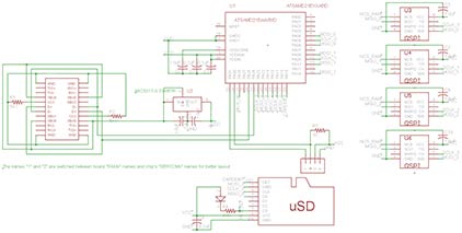
The first revision of the board had two memory chips, each on its own SPI bus, an SD card on the SPI bus, and USB with the appropriate resistors. The USB was perfect. Unlike everyone and their grandma (STMicro, I’m looking at you), Atmel didn’t license the pesky Synopsis USB IP. They made their own. It’s easy to use, elegant, and works well. Seriously, it just worked. In two days I got the hardware working and wrote a USB device stack. Hats off to the team that worked on the USB controller. However, I have a concern. My main problem: USB handles are not small. They are persistent. I would prefer to store them in flash. I would, but I can’t. The USB block uses the built-in DMA block to read data to send. This DMA block CAN access the flash, but if you have any flash wait states enabled, it sends garbage. I suspect Atmel tested it only for reads from RAM, forgot that some memories have wait states, and didn’t take that into account. Storing all my handles in RAM is a colossal waste of RAM, which is only 8KB. Remember that hair hat? I’ve scrapped it, Atmel. I had to work around this by sending the handles one at a time (instead of letting the direct network access hardware do it all automatically), just to save valuable RAM.
Using the SPI blocks directly worked pretty well until I tried to speed them up. After about 18 MHz, the data I received was garbled (one or two bits dropped, all subsequent bits shifted). No search found any problems in my code, and all the sample code did more or less the same thing. My bus analyzer didn’t find any problems. What does it do? IT DOES (archived)! I was furious when I found this forum post. Here I was trying to build a fast device, and my SPI bus was supposed to be limited to the speed of a tired snail calmly strolling through peanut butter! After some more testing, I found that the SPI blocks would work fine up to about 16 MHz, which I’ll have to live with.
SPI devices don’t have a FIFO, so the code has to manually send them one byte at a time and read them one byte at a time. This means there’s a gap between bytes on the bus as the code moves bytes to and from registers and memory. This is a waste of potential speed. The solution is DMA. Luckily, this chip has DMA. Unfortunately, it’s incredibly buggy, to the point where I’m starting to suspect that some sleep-deprived lunatic designed it.
A typical DMA device has a minimal global configuration and multiple channels, each independent of the rest. Each channel typically has a source address, a destination address, a length, and some configuration to store things like the transfer block size, the trigger, interrupt enable bits, etc. So, it’s common practice in ARM microcontrollers for each channel to have exactly these 4 32-bit configuration registers: SRC, DST, LEN, CFG. That’s 16 bytes of SRAM per channel. The ATSAMD21 has 12 DMA channels, so that would be 192 bytes of configuration data for the DMA device in total. Not much. Well, Atmel didn’t do anything about it! Instead, the device itself just has a POINTER to where in user RAM all this configuration data is. For each transfer, the DMA device loads its internal state for the active channel from this structure in RAM, and then operates on the channel. If the other channel’s data has already been loaded, it will be written to RAM first. Depending on your level of experience, you may be hearing your third or fourth “oh hell no” as you read this…
Why is this bad? Imagine two SPI devices powered by DMA. Each will have two DMA channels, one for receiving, one for transmitting. There will be four channels active in total. What happens when both SPI devices are powered up? The two DMA (transmitting) channels will become active and try to send a byte. One will go first, then the other. This will generate 14 (!!) bus transactions to RAM! Four to read the configuration data for one channel, one to read the byte to send, four to write that configuration data, four to read the configuration data for the next channel, and one more to read the byte to send. So, to send 2 bytes, the DMA device made 14 RAM accesses. Not great. But wait… that’s not all. Let’s see what happens next, when the SPI devices finish sending this byte and commit the received byte, but are also ready to send the next byte! At this point, only four bytes need to be logically moved (two from the devices to the receive buffers, two from the transmit buffers to the devices). Let’s see how that works. Remember that the DMA device’s internal configuration data is currently loaded onto the second transmit channel. First it will need to do 4 writes to output this data, then 4 reads to load the structures of the first receive channel, one write to memory to write the received byte to RAM, 4 writes to output the structures of that channel, 4 reads to load the structures for receive channel number 2, one write of the received byte to RAM, 4 bytes to write the configuration structure for that channel back to RAM, and then 14, which we already discussed, to send the next two bytes. This gives 36 RAM accesses to simply read two bytes and write two bytes. All this hassle, just to save transistors on the 192 bytes of SRAM that the DMA block would need to store all the configuration data internally.
So why is this bad? Let’s say our microcontroller is running at a design speed of 48 MHz and its SPI blocks are running at a design maximum speed of 12 MHz. By the time we need to send the second byte and receive the first received byte, we will need to make 36 RAM accesses and 4 SPI block accesses. The SPI block is on the APB bus, which means that any access to it takes at least 4 cycles. This means that between each byte sent and received, we will need 36 + 4 * 4 = 52 cycles. If the SPI block is running at 1/4 the speed of the processor, it will send/receive a byte every 8 * 4 = 32 cycles. So, every 32 cycles, we will need to do 52 cycles of work. When they don’t get enough cycles, the DMA channels give up and stop working… Oops…
So what can we do? I developed a hybrid method where I send data using a CPU write and receive it using Direct Memory Access (DMA). This worked for two channels, but not for more. Once I got the rev2 boards with 4 RAM chips, even that failed because only 4 DMA blocks for receiving were depriving each other of bandwidth and were canceled. Why was Atmel so stingy with internal SRAM? We’ll probably never know. But they could have solved this problem more easily than with 192 bytes of SRAM in the DMA block. Just adding 4-byte FIFOs to the SPI blocks would also make a difference, then each DMA transaction could transfer more than one byte, which would reduce this congestion. Unfortunately, apparently no one at Atmel even tried to actually use their chip for anything. Atmel, what happened to you?
My timing problems didn’t end there. This chip has several internal oscillators, one of which is supposed to be a fairly accurate 32 kHz oscillator called OSC32K. I wanted to use it as a clock source for a timer to implement my virtual real-time clock. Well, despite a lot of effort and a lot of tears, that damn clock never started… ever. The code should be simple: SYSCTRL->OSC32K.bit.EN32K = 1; SYSCTRL->OSC32K.bit.ENABLE = 1; while (!SYSCTRL->PCLKSR.bit.OSC32KRDY); Well… it didn’t. Eventually, I decided that I could use the less accurate OSC32KULP to clock my timer. It started, and I was able to use it. At this point in the project I was exhausted, desensitized to the many flaws of this chip, and completely out of it, so I resigned myself to the somewhat inaccurate real-time clock and continued working.
There’s not much to say about SD card support. Been there, done that, got the t-shirt. My initial prototype code used multi-block read/write for better card access speed, but in the final prototype I had to abandon this because one of the RAM chips on the b2 boards shared an SPI bus with the SD card, so leaving the card selected was impossible. This wasn’t that big of a deal, as SD card access is rarely, if ever, a bottleneck. Any card up to 2TB is supported.
In the v2 version of the board, I connected the card detection pin to the microcontroller. It wasn’t used, but I thought I might find a use for it. I didn’t, so it was removed in the v3 boards. I also added a card “activity” LED that lights up when the card is accessed. It’s just an LED between the card’s chip select line and Vcc. Whenever the card is selected, it’s on. This LED also serves a second function. If the SD card or SPI SRAM fails to initialize during boot, the system will output an error code to help identify the problem.
Now that the prototype is up and running and I’m making a layout for the final version, I decided to do something to make it look cool. I buried all the traces in layers 2 and 3, leaving layers 1 and 4 as continuous copper. It looks super cool! Of course, the top layer of copper is interrupted for the actual SMT pads, but other than that, everything is perfectly smooth and looks awesome!